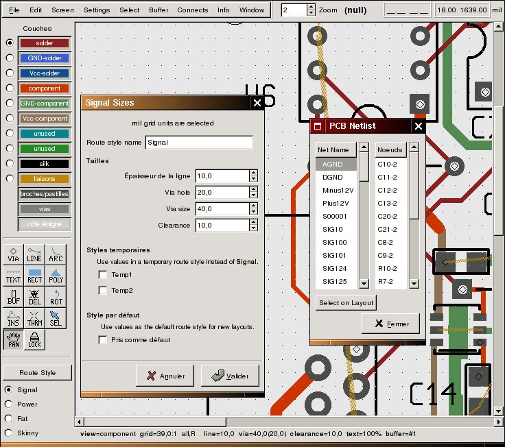
Le Sat, 26 Feb 2005 17:43:18 -0600
Bill Wilson <billw@xxxxxxxxxxxxxx> a écrit :

[cut]

> Don't know much about the .texi, but the tarball uploaded now has
> a pcb-gtk/po/pcb.pot file that you can start with.  I did add i18n to
> most of what I did.  Some of the popup confirms and other things
> probably are missed and I doubt the configure system is set up to
> enable i18n.
>
> Maybe you could succeed "by hand".  After the configure you would
> have to edit the src/Makefile and change the DEFS line to:
>
> DEFS = -DHAVE_CONFIG_H -DENABLE_NLS -DPACKAGE=\"pcb\"
-DLOCALEDIR=\"/usr/share/locale\"
>
> Then do a make.  And again by hand install the fr.po you have created:
>
>    cd src/po
>    msgfmt -f -v -o fr.mo fr.po
>    cp fr.mo /usr/share/locale/fr/LC_MESSAGES/pcb.mo
>
> Maybe it's better to wait until the PCB build can do it all for you,
but while
> I know what to do, I don't know how to make the autobuild tools do it.

I've done it manually as you suggest with some interesting results:

It works for additional opened windows as show on the screenshot but
don't for up selection bar nor for some layers: solder, GND-solder,
Vcc-solder, component... which aren't even in the .pot name list

and I have this error:


(pcb-bin:30381): Gtk-CRITICAL **: gtk_text_buffer_emit_insert: assertion
`g_utf8_validate (text, len, NULL)' failed

BTW, I join the fr_FR.po partially done too.

But it is really avery good job and enhance really pcb! ;-)

Cordially.


>
> Bill
>
>


--
Sur http://www.iznogood-factory.org , vous avez parmi des
doc techniques en français, celle de cinglés qui développent
des outils pour les schémas électroniques: gEDA.
Attachment:
fr_FR.po
Description: Binary data
Attachment:
pcb.jpg
Description: JPEG image
Attachment:
pgpfCWJHbdWM8.pgp
Description: PGP signature