(This is a resend - previous send was rejected)
Folks -
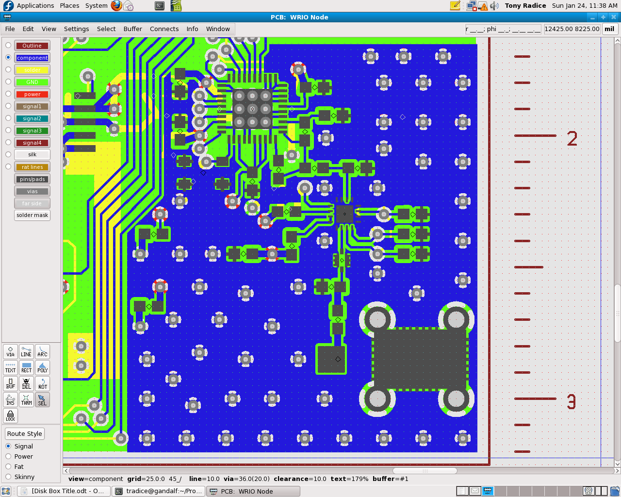
A solution I used for thermals on a surface mount set of components
- these are RF components that will ground to the surface layer on pin 2
(typically) of the footprint.
What I did was place a series of 10mil x 10mil square pads around
the perimeter of pad 2 such that there is 0 clearance between pad 2 and
the "thermal" pad, and 0 clearance between the thermal pad boundary and
the fill around the part. I am attaching a screen shot. The screen shot
has the silk layer turned off for clarity. The "trick" is figuring out
the exact coordinate location for the thermal pad itself. A little
pencil and calculator work, but here are the results. I also did
the same with a crystal (4 - pin rectangular) footprint, a filter
(that's the little goofy part in the center with the fingers outward),
and a custom antenna landing pad which had 28 of these suckers. If you
plan your parts symmetrically, this is rather easy.
Tony
Attachment:
Image-FcTRrI
Description: PNG image
_______________________________________________
geda-user mailing list
geda-user@xxxxxxxxxxxxxx
http://www.seul.org/cgi-bin/mailman/listinfo/geda-user