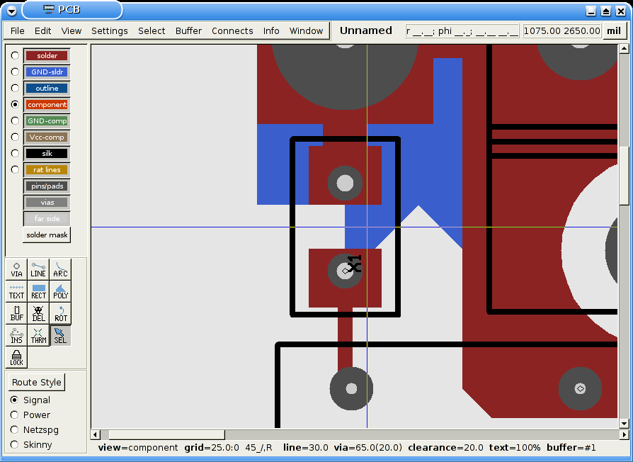
-----BEGIN PGP SIGNED MESSAGE-----
Hash: SHA1

Hi,

adding some final polygons to my layout, pcb (version 20091103) exhibits
some strange behavior regarding polygons. The polygon produces a short
circuit between the two pins. What's surprising, the filled area is
outside the contour I entered at one corner.

See the attached screenshot. The polygon causing the pain is blueish.

The PCB file to reproduce is attached as well.

When I enable thin draw poly mode, the outline of the polygon shown is
just as I want it to be. If pcb would fill only the region within the
contour, there would be no problem.

How can I work around that problem? I've been trying, but found no
working solution.

- - cl
-----BEGIN PGP SIGNATURE-----
Version: GnuPG v1.4.7 (GNU/Linux)
Comment: Using GnuPG with Mozilla - http://enigmail.mozdev.org

iD8DBQFL97NZWo2QgtqY4K8RAgkvAJ4+Sbr5/cr8jySVFVqsCpkGXajD7wCfYDvJ
w5Bq+ncEB6yABhG41ab1Msw=
=z2Qs
-----END PGP SIGNATURE-----
Attachment:
broken-poly.pcb.gz
Description: GNU Zip compressed data
Attachment:
screenshot.png.sig
Description: Binary data
Attachment:
broken-poly.pcb.gz.sig
Description: Binary data
_______________________________________________
geda-user mailing list
geda-user@xxxxxxxxxxxxxx
http://www.seul.org/cgi-bin/mailman/listinfo/geda-user