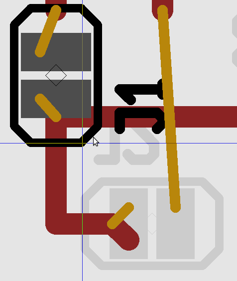
On Sun, 2010-10-17 at 14:50 +0200, Markus Hitter wrote:
Hello all,

yesterday I tried to replace a number of 2-pin jumpers (footprint
JUMPER2) with solder jumpers.
Of course, this should work fine, it does for me.
gsch2pcb removes the old footprints, but for my 2009 snapshot it
has not
put the new ones, you have to do something like "load element data to
buffer" to insert the new ones, and you may have to load the new
netlist
again. And you have to watch for the orientation of the new
footprints,
you may have to rotate them 180 degree. And press "O" key to update
ratsnest.
Did you make your layout with the autorouter? I have done all
manually,
so I am not sure if the autorouter needs special care when exchanging
footprints.

For replacing footprints there is a special mode which allows you to
replace single footprints -- sorry can not remember currently.
