[Author Prev][Author Next][Thread Prev][Thread Next][Author Index][Thread Index]
Re: gEDA-user: Gschem/PCB: how to deal with "special" pins & pads?
On Jul 23, 2010, at 1:28 AM, Richard Rasker wrote:
> Op woensdag 21-07-2010 om 16:35 uur [tijdzone -0400], schreef DJ
> Delorie:
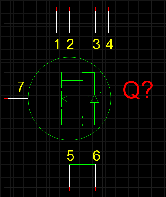
>>> - Internally connected pins and pads, e.g. SO8 MOSFETs with
>>> S on pins 1-3, G on pin 4, and D on pins 5-8. I can of course create a
>>> GSchem symbol with 3 pins for S and 4 pins for D, but is there a more
>>> elegant way in GSchem to deal with this?
>>
>> You could create a special S08 footprint with the pins numbered to
>> match the symbol, rather than have a symbol that's numbered to match
>> the generic footprint.
>
> Of course, that is a far better solution -- now why didn't I think of
> that? :-)
If you share the schematics with a group of folks for review and for diagnostics, it is a bad idea.
Every electrical engineer on the planet knows the standard so8 footprint. if you start numbering it differently then you will get confused people working on your design.
The safest approach is to call out each pin in the schematic, and use the SO8 standard footprint. You can make this look a bit prettier if you like, but you get the point.
Another option would be to patch the gschem -> pcb workflow to accept a list of pin numbers in the pinnumber attribute.

That is you would have one graphical pin with x electrical connections.

pinnumber=1,2,3,4


DJ:  could you add this to the import schematics feature of PCB?

>
>>> - So-called "don't care" pins and pads, e.g. mounting pads for SMD
>>> connectors.
>>
>> I name them "M1" through "M4" for example, and if you want to connect
>> them to something, yeah, they need to be in the netlist.  I'm not sure
>> if DRC ignores them if they don't *have* a name, though.
>
> I just tested this, but DRC checking doesn't appear to take pin naming
> into account.
>
>>> - Pure holes (e.g. for plastic positioning nubs of SMD connectors):
>>> these often fail DRC check when too close to copper surfaces (e.g.
>>> mouting pads) -- probably because mounting holes are genarally used
>>> with metal screws.
>>
>> DRC doesn't know about screws, it only knows its rules, and even pure
>> holes should obey them or they might short.
>>
>>> Am I correct in surmising that gEDA currently only accomodates type 1?
>>
>> #2 can be done just by giving all the "same" pin the same name/number.
>
> So I figured already. Anyway, thanks for clearing things up, it will no
> doubt make working with gEDA even more enjoyable.
>
> Best regards,
>
> Richard Rasker
>
>
>
> _______________________________________________
> geda-user mailing list
> geda-user@xxxxxxxxxxxxxx
> http://www.seul.org/cgi-bin/mailman/listinfo/geda-user
_______________________________________________
geda-user mailing list
geda-user@xxxxxxxxxxxxxx
http://www.seul.org/cgi-bin/mailman/listinfo/geda-user