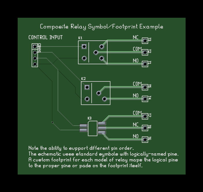
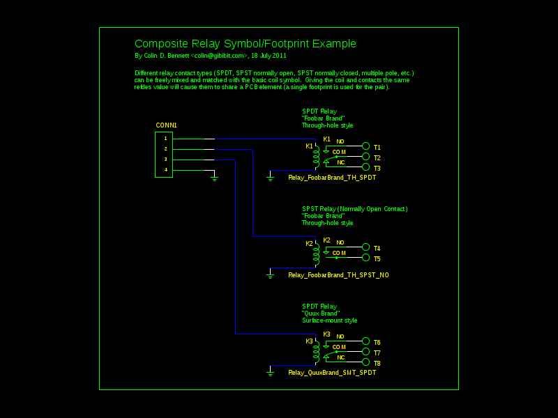
On Fri, 15 Jul 2011 21:25:53 +0200
Hans Schulz <hans@xxxxxxxxxxxxx> wrote:

> As sort of an extension to heterogeneous symbols I wonder how I can
> make generic symbols, consisting of a set of "sub"symbols, e.g. a
> relay coil and several types of contact arrangements like SPST and
> SPDT, all as separate, little symbols. In my design I would then
> select the appropriate subparts and assemble a particular
> arrangement, assign the same refdes to them (probably suffixed by
> "a", "b", "c" or similar in lower case). So far this is simply
> possible with gschem AFAIK. BUT: relays (to stick to the example)
> come in (very) many different physical shapes and layouts, each with
> its own, vendor dependent pin numbering scheme. Therefore, it would
> be nice to have the possibility to define the pin numbers in the
> instantiation at the schematic level rather than the fixed pin
> numbers as defined in the symbol (class level). The slot mechanism is
> not intented nor useable for this. I have not found any way to
> promote the pinnumbers to the instantiation or other ways to achieve
> this.

I hacked together a quick example that might help you.
Suppose you wanted to support both SPST and SPDT relays in various
physical configurations.  The goal is to avoid creating a schematic
symbol for each specific relay model.

Instead of a symbol for each relay model, we let symbols remain purely
logical entities and put the logical-physical mapping directly inthe
footprint.

Create a symbol for each of the following:
- Relay coil
- Relay contacts for SPDT relay
- Relay contacts for SPST (NO) relay

In each of the symbols, you DO NOT use physical pin names/numbers, but
instead use a logical name/number from the following scheme:

Coil:
- COILA
- COILB
Contacts:
- COM
- NO
- NC
(for multiple-pole relays, you could add COM2, NO2, etc.)

Then you simple create footprints for the specific relay in use, where
the pcb footprint pin/pad name matches the proper logical name from the
schematic symbol.  I generally end up creating a footprint myself for
nearly every component anyway, so this is no extra work.  You could
easily copy and modify an existing relay footprint, as well.

Check out the attached schematic and PCB images to see how it could be
implemented.

Find the source at
<http://gibibit.com/upload/2011-07-18_CompositeRelaySymbols.zip>.

I used a separate symbol for the coil and for the set of contacts, but
you could integrate these if you don't have too many variants (then you
don't have to match the two refdes's), or if you have TONS of wacky
variants you could try to create separate symbols for each contact
terminal, but I doubt that would be worth it.  Just copy and modify the
standard SPDT contacts for each custom configuration.

Regards,
Colin
Attachment:
Test_Relay_Board.png
Description: PNG image
Attachment:
Test_Relay_Circuit.png
Description: PNG image
_______________________________________________
geda-user mailing list
geda-user@xxxxxxxxxxxxxx
http://www.seul.org/cgi-bin/mailman/listinfo/geda-user