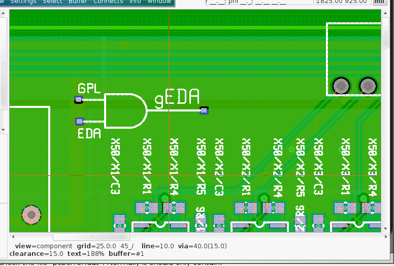
I've knocked up a gEDA logo for dropping onto PCB boards. Since I can't
save text in the element, this is actually a .pcb file.

The gEDA logo makes use of an element so it can have soldered pads for
the nodes of the gEDA AND gate.

Why not include this on your next gEDA board.

(BTW.. I'm counting PCB as part of gEDA, so didn't use a separate logo
for that).


Enjoy!

--
Peter Clifton

Electrical Engineering Division,
Engineering Department,
University of Cambridge,
9, JJ Thomson Avenue,
Cambridge
CB3 0FA

Tel: +44 (0)7729 980173 - (No signal in the lab!)
Attachment:
geda_logo.pcb
Description: application/pcb-layout
_______________________________________________
geda-user mailing list
geda-user@xxxxxxxxxxxxxx
http://www.seul.org/cgi-bin/mailman/listinfo/geda-user