Dear All,
This is my first post, so hello & thanks to those who
provide/support the mailing list. In my last project, PCB was acting
strangely - some of the time. I can't seem to recreate this problem,
but I suspect that I had set a setting wrong or something so I thought
I'd send it to the list for clarification.
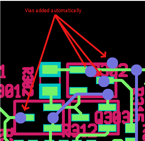
Whenever a net was selected, all other unrouted pads would have a
via placed on top of them, routed nets did not do this. I could undo,
and I found that restarting PCB seemed to solve it, but the problem
happened a number of times and lead to a mistake in the design that
would been built, if my PCB manufacturer hadn't flagged it [see
image]. I would guess that it was me accidentally setting some
auto-routing feature with a shortcut key, however knowing what it is
would be invaluable to avoiding this problem in future.
I am using version "20080202, Compiled on Feb 13 2008 at 21:19:20,
by harry eaton", the board was 4 layers thick, everything else seemed
to be as standard. I'm sorry that I can't give more detailed
information about the when the issue appeared.
I apologise if this has been discussed before - I've googled for it
but don't know exactly what you'd call this behaviour.
Andrew
--
╒═════════════════════════════════════════════╕
Andrew Whyte MEng CEng
Electronics & Software Design Engineer
╘═════════════════════════════════════════════╛
Attachment:
capture.png
Description: PNG image
_______________________________________________
geda-user mailing list
geda-user@xxxxxxxxxxxxxx
http://www.seul.org/cgi-bin/mailman/listinfo/geda-user