On Thu, May 19, 2011 at 4:25 PM, Colin D Bennett <[1]colin@xxxxxxxxxxx>
wrote:
On Thu, 19 May 2011 14:02:58 -0400
Vanessa Ezekowitz <[2]vanessaezekowitz@xxxxxxxxx> wrote:
> The discussion about "reinventing the wheel" reminded me:
>
> The TO92 footprint included with PCB does not work with the schematic
> importer therein. Try to reference it and the importer complains
> about missing pins, because it uses numbered pins instead of the
> B-C-E lettering used in gschem's transistor symbols. Copy and edit
> the footprint to use those letters and the importer complains about
> pin numbers ending in letters.
Isn't a word of caution in order, since not all TO-92 transistors
use
the same order of B/C/E pins?
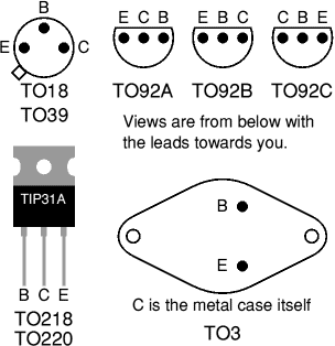
Yes, I think there is supposed to be a TO-92A, TO-92B, and TO-92C (the
different orders) but nobody paid enough attention, and I'm not sure if
this is standard, or merely convention. see attached gif that was
stolen from
[3]http://www.kss.sd23.bc.ca/chalmers/robotics10/Labs/ComparePNPNPN/how
Explained.htm
References
1. mailto:colin@xxxxxxxxxxx
2. mailto:vanessaezekowitz@xxxxxxxxx
3. http://www.kss.sd23.bc.ca/chalmers/robotics10/Labs/ComparePNPNPN/howExplained.htm
Attachment:
tranlead.gif
Description: GIF image
_______________________________________________
geda-user mailing list
geda-user@xxxxxxxxxxxxxx
http://www.seul.org/cgi-bin/mailman/listinfo/geda-user