Friends -
Can I call your attention to the disturbingly inconsistent state of
affairs regarding simple passive footprints in pcb? And BTW, my
conversations with other ECAD users suggests the problem is not
unique to this software. All dimensions below are in mils (sorry).
AVX 0603 part dimensions:
length 63 +/- 6
width 32 +/- 6
terminal 14 +/- 6
Panasonic 0603 part dimensions:
length 63 +/- 4
width 31 +/- 4
terminal 12 +/- 8
not_vetted_ingo smt0603.ele
length 91
width 30
terminal 31
gap 29
~geda geda_0603 Standard SMT resistor, capacitor, etc
length 72
width 42
terminal 24
gap 24
~generic smd_capacitor_603 chip_capacitor
length 90
width 40
terminal 30
gap 30
~generic generic_smd_chip_603 smd chip 603
length 60
width 30
terminal 14
gap 32
~genericsmt SMT_603_CAP_RES SMT 603 type capicitor/resistor
length 70
width 39
terminal 17
gap 36
footgen
length 87
width 32
terminal 28
gap 31
Average (after removing extrema)
length 80
width 35
terminal 25
gap 30
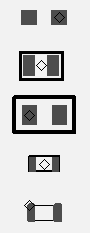
The first five footprints (in order, from not_vetted_ingo to ~genericsmt,
top to bottom) are displayed in the attached PNG (if your mail system
mangled it, you can see this file at
http://recycle.lbl.gov/~ldoolitt/caplist.png
). These footprints are all included in pcb snapshot 20040903, and I
don't think anything relevant changed for 20050609. I ignore, for now,
the equally dramatic differences in center position and silkscreen.
Of course, other sizes (0402, 0805) are similarly inconsistent.
While I know some simple stuff, like those 60 and 70 mil long footprints
would make it a bear to hand-solder a part that's 60 mils long. I suspect
a lot of people here have more first-hand experience as to what makes a
good SMT footprint. Can you share it with me?
More generally, does anybody have a plan for systematizing and vetting the
pcb footprint library? The "newlib" part of PCB seems to go one direction,
and my qfp-ui and Darrell Harmon's footgen go quite another. Can we keep
and expand both? My goal would have the following:
- on-line database of footprints, with tracking of modification history
- clear separation of, but cross-index between, footprints and chip
part numbers
- on-screen "wizard" interface to edit and create footprints
* better interface than qfp-ui
* more geometries than footgen
* simple user option to submit result to on-line database
- 90% of the legacy crud removed from default pcb installs
Thanks for your attention!
- Larry
Attachment:
caplist.png
Description: PNG image
Attachment:
signature.asc
Description: Digital signature