[Author Prev][Author Next][Thread Prev][Thread Next][Author Index][Thread Index]
gEDA-user: pcb crooked traces
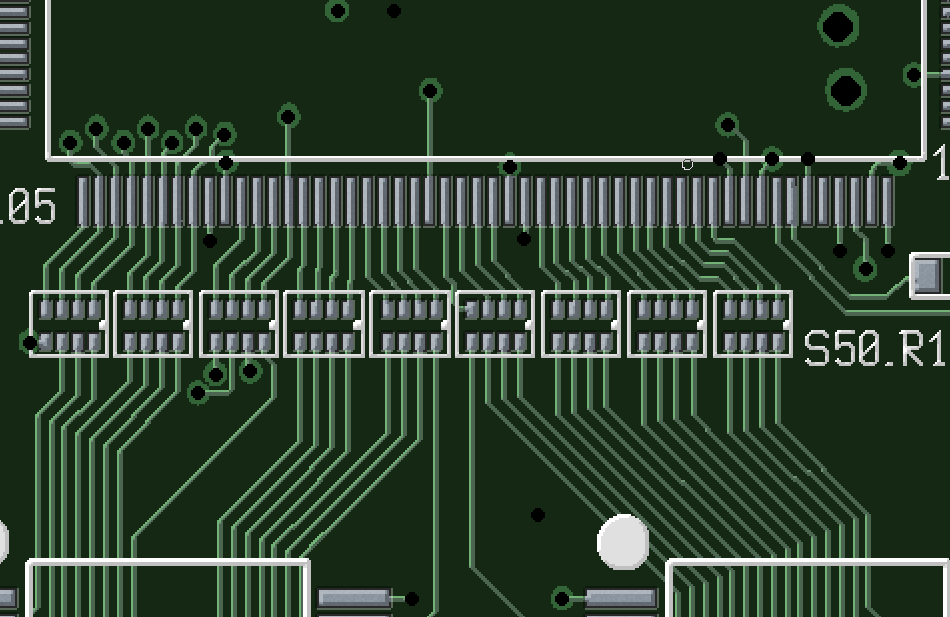
I hope the attachment comes through. If not, I'll post it somewhere.
I cannot get rid of the jagged diagonal lines on my design. There's
lots of them. The picture shows a couple of examples. I've tried
different grid sizes, line widths, but nothing fixes the problem.
Redrawing them in order to eliminate any sections does not help. On
PCB, it shows at some zoom levels but not others. It is in the gerbers
as well and it is in the photo-mode picture I attached.
PCB 2009


It passes my design rules, but looks ugly.

Traces are 8 mil, spacing is 8 mil.  Grid space is 1 mil.

gene
_______________________________________________
geda-user mailing list
geda-user@xxxxxxxxxxxxxx
http://www.seul.org/cgi-bin/mailman/listinfo/geda-user