[Date Prev][Date Next][Thread Prev][Thread Next][Date Index][Thread Index]
Re: [f-cpu] Re: FC0 XBAR
hi,
Juergen Goeritz wrote:
> > > we CAN detect when the bank is accessed both for read and write.
> > > we can even delay the instruction that does that (but it's not desirable).
> > > however, on some cases it might be that the hardware doesn't need
> > > such a measure. it depends too much on the silicon characteristics...
> >
> > If there is a read-after-write dependency, we have to a) bypass the
> > result of the first instruction (if the result arrives in time) or b)
> > delay the second instruction (if bypassing is not possible or the result
> > ist NOT ready).
>
> Maybe I didn't get it yet!? Aren't you guys designing synchronous
> computing units with registered outputs? Handling the transfer
> back to the register bank in the next clock? Thus having a
> pipeline of decoding->read_from_reg&exec->write_to_register->...?
> Could someone point me to my misunderstanding please?
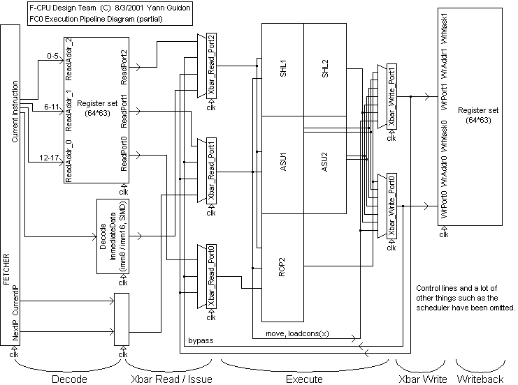
i'll have to make a "little drawing", now ...
<2 hours later ...>
ok i've done a little sketch.
you will understand why it is called "superpipeline" because execution occurs
2 cycles after the register read has started. As i told you one day, F-CPU
is not your "average CPU core" :-)
Due to the already complex drawing, i have not included the scheduler
and other control signals. Even the wire names are not acurate.
I have included 3 execution units only. However it gives a rough
idea about how it is designed. You can now read the QDCPOC source code
with the (partial) map under your eyes.
> JG
WHYGEE
~~~~~~~~~~~~~~~~~~~~~~~~~~~~~~~~~~~~~~~~~~~~~~~~~~~~~~