Igor2 <igor2@xxxxxxxxxxx> wrote:
> On Sat, 22 Dec 2007, DJ Delorie wrote:
>
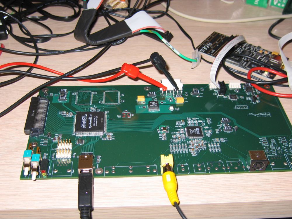
>>
>>> http://ad7gd.net/geda/panelusb-sm.jpg
>>
>>Am I the only one who tries to make the absolutely smallest board I
>>can still fit my parts on? My latest board would fit in the blank
>>spots between your chips.
>
> I do that too - saves cost but it's bad when I have to debug or replace or
> add parts.
>
> Btw, how do you guys solder those big SM chips with so many pins? I've
> just bought a chip with TQFP64_10, managed to iron and etch a board for it
> but I am still not sure how I would solder the chip.
Reflow oven + solder paste.
http://web.interware.hu/lekovacs/reflow_oven/index.html
--
Levente
http://web.interware.hu/lekovacs
_______________________________________________
geda-user mailing list
geda-user@xxxxxxxxxxxxxx
http://www.seul.org/cgi-bin/mailman/listinfo/geda-user
_______________________________________________ geda-user mailing list geda-user@xxxxxxxxxxxxxx http://www.seul.org/cgi-bin/mailman/listinfo/geda-user