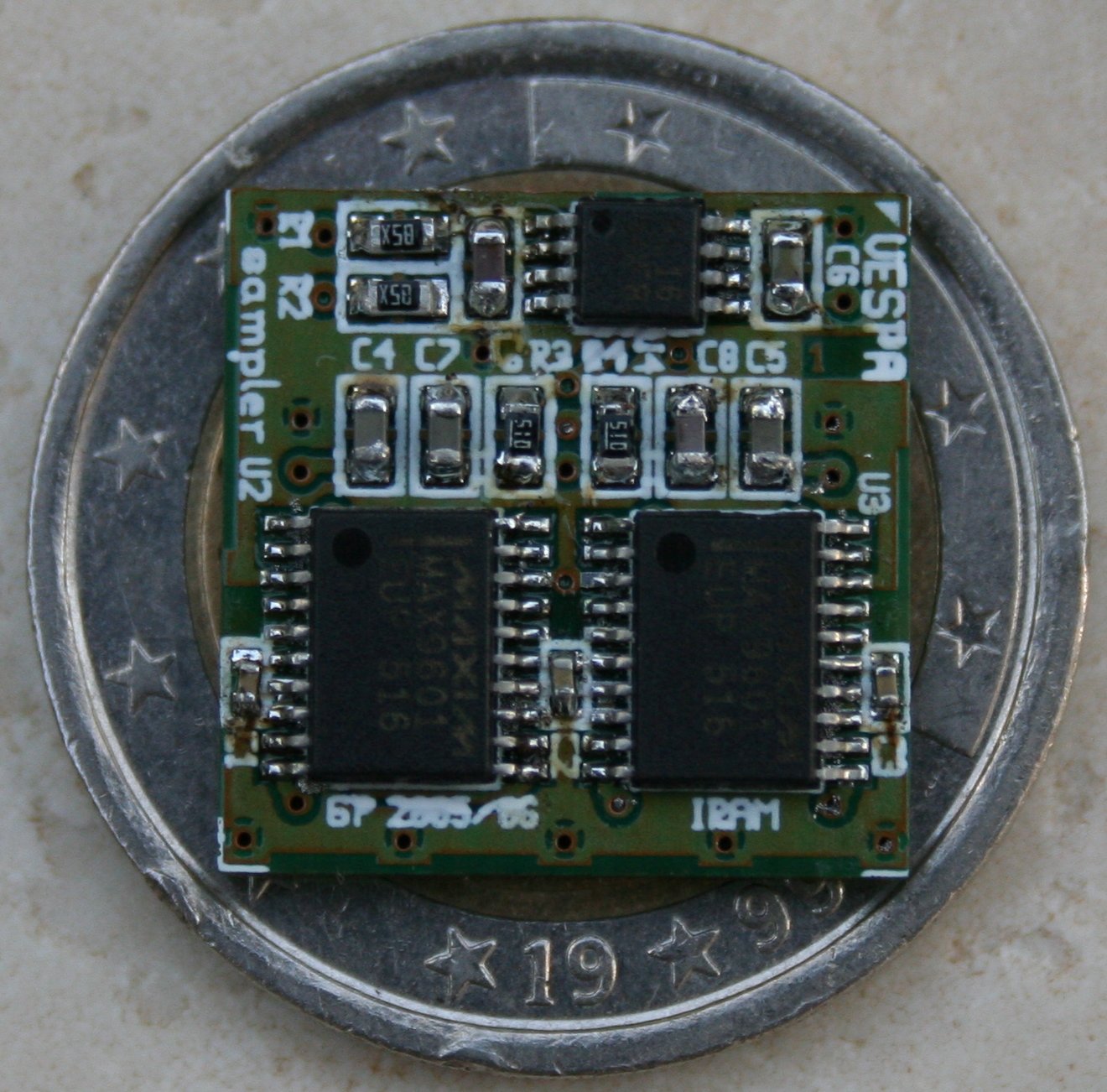
On Mon, Mar 09, 2009 at 08:09:45AM -0400, John Luciani wrote:
> On Mon, Mar 9, 2009 at 7:39 AM, gene <carzrgr8@xxxxxxxxxxxxx> wrote:
>
> > How small can the font be made before it becomes unreadable?
>
> How thin a line can your PCB vendor draw? IIRC the specs at
> PCB Express and Advanced Circuits are line widths of 10mils width
> and spacing of 10mils. I believe the default character height in
> PCB is around 50mils. I would be surprised if you could go
> much smaller than 40mils (with 10/10 rules).

The default in PCB is 45mil, whatever it means. In 2005 I did
a small board to replace a completely obsolete chip (SP93804)
in a critical system here. To fit all the text I reduced the
size of refdes to 27mil in PCB, and they were drawn with 6mil
lines IIRC. The attached picture gives you an idea of how it
looks (it's the prototype which I hand assembled and it shows,
but the 4 layer PCB was obviously subcontracted), not all
characters are really readable.

	Gabriel
Attachment:
Sampler.JPG
Description: JPEG image
_______________________________________________
geda-user mailing list
geda-user@xxxxxxxxxxxxxx
http://www.seul.org/cgi-bin/mailman/listinfo/geda-user