Dave,

This is crude and might not make the solder paste gerber files
correctly.

But it gets my idea across.

Steve Meier


On Tue, 2008-03-11 at 10:39 -0800, Dave N6NZ wrote:
> Ben Jackson wrote:
> > You've always had to draw lines to pads to connect to any
> > surface polygons.
>
> Not being able to create non-round pins that support thermals is a
> fundamental brokenness.  Let's fix it.
>
> -dave
>
>
>
> _______________________________________________
> geda-user mailing list
> geda-user@xxxxxxxxxxxxxx
> http://www.seul.org/cgi-bin/mailman/listinfo/geda-user
Attachment:
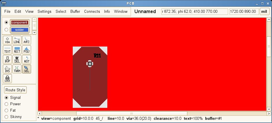
pin_pad_polygon.jpg
Description: JPEG image
Attachment:
test.pcb
Description: application/pcb-layout
Element(0x00000000 "" "R11" "" 1800 1050 56 -138 0 100 0x00000000)
(
	Pin(0 0 60 30 60 28 "" "1" 0x00000001)
	Pad [ 0     0    0    35000 10000 10000 45000 "1" "1" 0x00000100]
)
_______________________________________________
geda-user mailing list
geda-user@xxxxxxxxxxxxxx
http://www.seul.org/cgi-bin/mailman/listinfo/geda-user