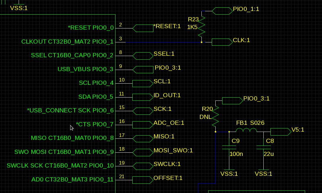
On Mon, May 2, 2011 at 10:49 AM, Peter Clifton <pcjc2@xxxxxxxxx> wrote:
> On Sun, 2011-05-01 at 19:23 -0500, David W. Schultz wrote:
>> On 05/01/2011 07:01 PM, Stephen Ecob wrote:
>> > Are there any gschem oldtimers around who can explain the rational for
>> > the :1 requirement ?
>> > If there's no good reason for it I'd be happy to write a patch that removes it.
>>
>> I am not an old timer but I believe that this is required to attach that
>> net name to pin 1 of the symbol. The net name doesn't actually include
>> the :1.
>
> Exactly right - and there is a reluctance (certainly from me) to create
> special cases where that attribute can be dropped for single pin
> symbols.
>
> I'm quite keen to see John Dotty's suggestion (or a variant of it)
> implemented though.

Thanks for the explanation guys.  John Doty's suggestion does sound
good - using David's example:

net:28=Vcc
T 300 6750 5 10 0 0 0 0 1
net:14=GND
T 300 5750 9 10 1 0 0 0 1

is (to me) cleaner than:

net=Vcc:28
T 300 6750 5 10 0 0 0 0 1
net=GND:14
T 300 5750 9 10 1 0 0 0 1

For me the main problem, though, is the visual clutter in my
schematics when using lots of inputs and outputs.  I've attached a
screen grab of a particularly cluttered part of one of my recent
schematics.
Attachment:
Screenshot.png
Description: PNG image
_______________________________________________
geda-user mailing list
geda-user@xxxxxxxxxxxxxx
http://www.seul.org/cgi-bin/mailman/listinfo/geda-user