[Author Prev][Author Next][Thread Prev][Thread Next][Author Index][Thread Index]
Re: gEDA-user: pcb flip-sides
On Thu, 2009-10-29 at 14:30 -0400, DJ Delorie wrote:
> > I got very (very) ((very)) confused by the code. Since everything is
> > indexed by the same range of numbers, it is easy to make mistakes. I
> > suspect I have made mistakes..
>
> For a physical stackup, you want to iterate through the layer groups,
> not the layer stack.  For each group, draw all the layers in that
> group.

Ok, got it. Looks like I was doing that wrong:


The layer stack deals in _layer_ number
"group" is the layer _group_ to render

I think the layer stack confused me. (layer stacks, layers, layer groups)!

BTW: order_i is an iterator from 0-maxlayers-1:

   for (ngroups = 0, i = 0; i < max_layer; i++) {
     int orderi = reverse_layers ? max_layer - i - 1 : i;

-    group = GetLayerGroupNumberByNumber (global_view_2d ? LayerStack[i] : orderi);
+    group = global_view_2d ? GetLayerGroupNumberByNumber (LayerStack[i]) : orderi;
                                                     ^__ LAYER NUMBER, RIGHT?
     ...
   }

(^__ ABOVE IS PROBABLY STILL WRONG!)


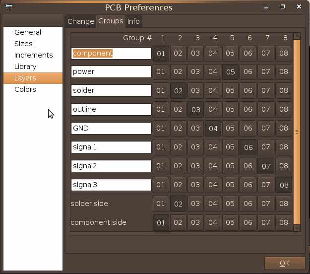
I think the "bug" I was seeing relates to how the GTK HID (at least -
not sure about lesstif), moves layers. I move a layer, in this case
"power", up to what _appears_ to be just underneath the solder layer,
but in fact this happens to the layer groups:

"power" remains as layer group 5, but swaps into _layer_ number 2. (See
attached image)

I guess either I need to get it to shuffle the groupings as well as the
layer numbers, and probably look at how the loop iterates.. and what to
render, when "solder side" and "component side" are on odd layer group
numbers.

By rights, I suspect the default layer stack should just be rendered as
a 2 layer board.. since power, outline, GND, signal* belong to layer
groups outside the range of the solder and component group numbers.


Did I start to get that straight?

_______________________________________________
geda-user mailing list
geda-user@xxxxxxxxxxxxxx
http://www.seul.org/cgi-bin/mailman/listinfo/geda-user
